NCT7491
http://onsemi.com
4
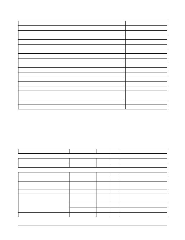
Table 1. ABSOLUTE MAXIMUM RATINGS
Parameter
Rating
Positive Supply Voltage (V
CC
)
3.6 V
Maximum Voltage on +12V
IN
Pin
14 V
Maximum Voltage on +5V
IN
Pin
6.25 V
Maximum Voltage on All OpenDrain Outputs (excluding PWM pins)
3.6 V
Maximum Voltage on PWM Pins
+5.5 V
Maximum Voltage on TACH Pins
+5.5 V
Voltage on Remaining Input or Output Pins
0.3 V to +4.2 V
Input Current at Any Pin
? mA
Package Input Current
?0 mA
Maximum Junction Temperature (T
J
max
)
150癈
Storage Temperature Range
65癈 to +150癈
Lead Temperature, Soldering
IR Reflow Peak Temperature
220癈
PbFree Peak Temperature
260癈
Lead Temperature (Soldering, 10 sec)
300癈
ESD Rating
HBM
2 kV
FICDM
0.5 kV
Stresses exceeding Maximum Ratings may damage the device. Maximum Ratings are stress ratings only. Functional operation above the
Recommended Operating Conditions is not implied. Extended exposure to stresses above the Recommended Operating Conditions may affect
device reliability.
Specifications
T
A
= T
MIN
to T
MAX
, V
CC
= V
MIN
to V
MAX
, unless
otherwise noted. All voltages are measured with respect to
GND, unless otherwise specified. Typical voltages are at T
A
= 25癈 and represent a parametric norm. Logic inputs accept
input high voltages up to V
MAX
, even when the device is
operating down to V
MIN
. Timing specifications are tested at
logic levels of V
IL
= 0.8 V for a falling edge, and V
IH
= 2.0 V
for a rising edge. SMBus timing specifications are
guaranteed by design and are not production tested.
Table 2. SPECIFICATIONS
Parameter
Min
Typ
Max
Unit
Test Conditions/Comments
POWER SUPPLY
Supply Voltage
3.0
3.3
3.6
V
Supply Current, I
CC
1.5
5
mA
Interface inactive, ADC active
TEMPTODIGITAL CONVERTER
Local Sensor Accuracy
?.5
?.5
癈
0癈 d T
A
d 85癈
Local Sensor Resolution
0.25
癈
Remote Diode Sensor Accuracy
?.5
?.5
癈
0癈 d T
A
d 85癈
40癈 d T
D
d 125癈
Remote Sensor Resolution
0.25
癈
Remote Sensor Source Current
30
mA
Low Level 1
240
mA
High Level 1
37.5
mA
Low Level 2
300
mA
High Level 2
Series Resistance Cancellation
270
W
发布紧急采购,3分钟左右您将得到回复。
相关PDF资料
NCT75MNR2G
IC SENSOR TEMP DGTL 8DFN
NCV8881PWR2G
IC REG TRPL BUCK/LINEAR 16SOIC
NE1617ADS,112
IC TEMP MONITOR 16SSOP
NE1619DS,118
IC TEMP MONITOR 16SSOP
NIS5112D1R2G
IC ELECTRONIC FUSE HOTSWAP 8SOIC
NIS5132MN2TXG
IC ELECTRONIC FUSE 12V 10DFN
NIS5132MN3TXG
IC ELECTRONIC FUSE 12V 10-DFN
NSI45015WT1G
IC LED DRIVER LINEAR SOD-123
相关代理商/技术参数
NCT75DMR2G
功能描述:板上安装温度传感器 2-Channel Digital Thermometer w/ Alarm
RoHS:否 制造商:Omron Electronics 输出类型:Digital 配置: 准确性:+/- 1.5 C, +/- 3 C 温度阈值: 数字输出 - 总线接口:2-Wire, I2C, SMBus 电源电压-最大:5.5 V 电源电压-最小:4.5 V 最大工作温度:+ 50 C 最小工作温度:0 C 关闭: 安装风格: 封装 / 箱体: 设备功能:Temperature and Humidity Sensor
NCT75DR2G
功能描述:板上安装温度传感器 2-Channel Digital Thermometer w/ Alarm
RoHS:否 制造商:Omron Electronics 输出类型:Digital 配置: 准确性:+/- 1.5 C, +/- 3 C 温度阈值: 数字输出 - 总线接口:2-Wire, I2C, SMBus 电源电压-最大:5.5 V 电源电压-最小:4.5 V 最大工作温度:+ 50 C 最小工作温度:0 C 关闭: 安装风格: 封装 / 箱体: 设备功能:Temperature and Humidity Sensor
NCT75MNR2G
功能描述:板上安装温度传感器 HAS2MONOJLCC84SPACE
RoHS:否 制造商:Omron Electronics 输出类型:Digital 配置: 准确性:+/- 1.5 C, +/- 3 C 温度阈值: 数字输出 - 总线接口:2-Wire, I2C, SMBus 电源电压-最大:5.5 V 电源电压-最小:4.5 V 最大工作温度:+ 50 C 最小工作温度:0 C 关闭: 安装风格: 封装 / 箱体: 设备功能:Temperature and Humidity Sensor
NCT7717U TR
制造商:Nuvoton Technology Corp 功能描述:SMBUS INTERFACE TEMP. SENSOR W 制造商:Nuvoton Technology Corp 功能描述:IC SMBUS TEMP SENSOR 8MSOP
NCT7718W TR
制造商:Nuvoton Technology Corp 功能描述:IC SMBUS TEMP SENSOR 8MSOP
NCT7802Y
制造商:Nuvoton Technology Corp 功能描述:
NCT7904D
制造商:Nuvoton Technology Corp 功能描述:IC H/W MONITOR
NCT80DBR2G
功能描述:板上安装温度传感器 RoHS:否 制造商:Omron Electronics 输出类型:Digital 配置: 准确性:+/- 1.5 C, +/- 3 C 温度阈值: 数字输出 - 总线接口:2-Wire, I2C, SMBus 电源电压-最大:5.5 V 电源电压-最小:4.5 V 最大工作温度:+ 50 C 最小工作温度:0 C 关闭: 安装风格: 封装 / 箱体: 设备功能:Temperature and Humidity Sensor
